Search...

Transistors operate in three modes: cutoff, active (amplification), and saturation. In digital applications, we typically use transistors in cutoff and saturation modes to function as electronic switches.
When base current Ib ≥ 1mA, the NPN transistor enters saturation mode:
The collector-emitter path conducts;
The collector voltage drops close to 0V (GND);
The load (RL) gets nearly full supply voltage across its terminals.
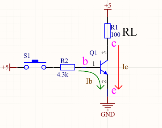
Figure 1: NPN Transistor Circuit
A pushbutton S1 provides ≈1mA base current. The emitter is grounded, and the load is placed between Vcc and the collector.
Note: The voltage drop between base and emitter (V_BE) is around 0.6–0.7V.
For a PNP transistor:
When the base voltage is pulled low (≈0.7V below emitter), and Ib ≥ 1mA, the transistor saturates;
The emitter-collector path conducts;
The collector voltage approaches Vcc.
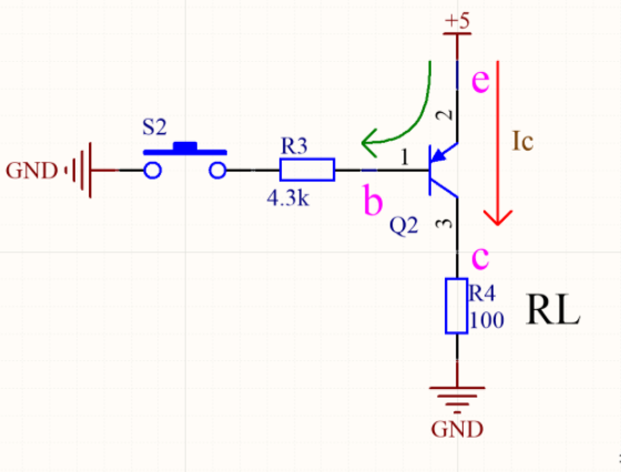
Figure 2: PNP Transistor Circuit
Pressing switch S2 provides ≈1mA base current. The emitter is connected to Vcc, the load is between the collector and GND.
To ensure fast turn-off and stable logic when input is disconnected:
Add a pull-down resistor (2kΩ–10kΩ) at the base.
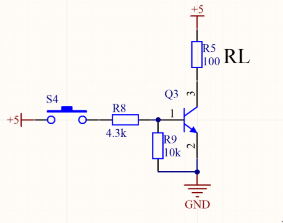
Figure 3: NPN Transistor with Pull-Down Resistor
This helps discharge the base-emitter capacitance and ensures the transistor remains OFF when no input is applied.
Same concept applies for PNP transistors:
Add a pull-up resistor (2kΩ–10kΩ) at the base to ensure complete cutoff
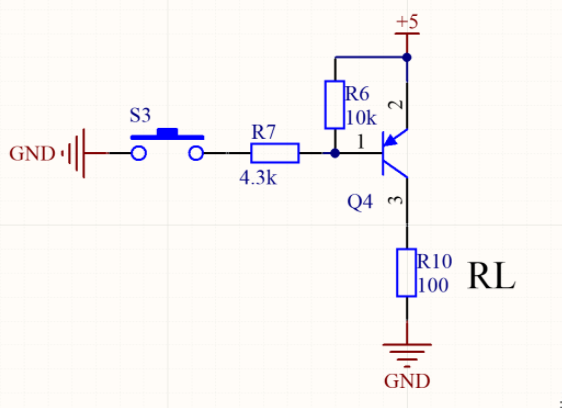
Figure 4: PNP Transistor with Pull-Up Resistor
Stabilizes base voltage and improves response time.
Inductive loads (e.g., relays, buzzers) generate high-voltage spikes when switched OFF. This spike can damage the transistor.
Use a flyback diode in reverse bias across the load to absorb the spike.
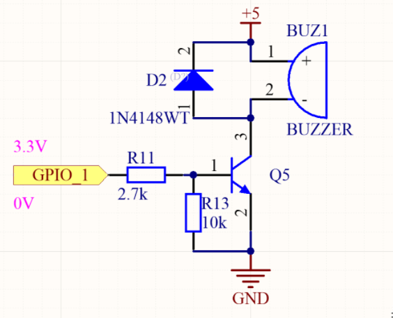
Figure 5: NPN Transistor Driving a Buzzer with Flyback Diode
The diode protects the transistor from reverse EMF. Fast recovery or Schottky diodes (like 1N5819) are recommended.
Some control signals may not pull the base fully to 0V. This can cause incomplete cutoff.
Add a forward diode or Zener diode at the base to raise the turn-on threshold.
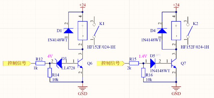
Figure 6: NPN Transistor Driving Relay with Clamping Diode
Useful with open-collector (OC) outputs, delayed signals, or diode-isolated signals. Avoid this for push-pull outputs.
This circuit enables:
Delayed turn-on using RC charging;
Fast shut-off via a discharge transistor path.
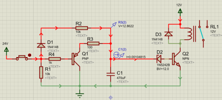
Figure 7: Transistor-Based Delay Control for Relay
When C1 charges to 12V, Q2 turns ON. Q1 helps quickly discharge C1 during turn-off.
V_BE ≈ 0.7V (NPN), V_EB ≈ 0.7V (PNP) to turn on;
Ib ≥ 1mA ensures saturation in small-signal BJTs;
Add pull-down (NPN) or pull-up (PNP) resistors on the base;
Always use flyback diode for inductive loads;
Add clamping diodes for noisy/uncertain logic inputs;
Design delay control with RC + transistor discharge path;
Assume β = 10–20 for switch mode, even if the datasheet shows β > 100.
 More information?
AXTEK Series NYQUEST CMSEMICON ST MICROELECTRONICS Featured Manufacturers Puya MCUs ICMAN Touch Chips ZXInfoTek Holtek MCUs MORNSUN Modules
Company Profile Certificates Terms & Conditions Privacy Statement


 MCU Solutions
 PCBA Solutions
 Bluetooth Solutions
 FAQ
FAQ Contact Us
 Company News
 Technology News
 Industry News
 PCBA News
 Company Profile
 Certificates
 Terms & Conditions
 Privacy Statement
 Home Appliances
 Beauty Appliances
 Lighting
 Kid's Toys
 Security Alarm
 Health Care
