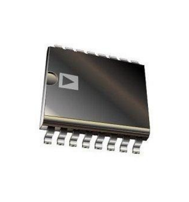
Description:
The AT25DF321A is a serial interface Flash memory device designed for use in a wide variety of high-volume consumerbased applications in which program code is shadowed from Flash memory into embedded or external RAM for execution.The flexible erase architecture of the AT25DF321A, with its erase granularity as small as 4-Kbytes, makes it ideal for datastorage as well, eliminating the need for additional data storage EEPROM devices.The physical sectoring and the erase block sizes of the AT25DF321A have been optimized to meet the needs of today's codeand data storage applications. By optimizing the size of the physical sectors and erase blocks, the memory space can be usedmuch more efficiently. Because certain code modules and data storage segments must reside by themselves in their ownprotected sectors, the wasted and unused memory space that occurs with large sectored and large block erase Flash memorydevices can be greatly reduced. This increased memory space efficiency allows additional code routines and data storagesegments to be added while still maintaining the same overall device density.The AT25DF321A also offers a sophisticated method for protecting individual sectors against erroneous or malicious programand erase operations. By providing the ability to individually protect and unprotect sectors, a system can unprotect a specificsector to modify its contents while keeping the remaining sectors of the memory array securely protected. This is useful inapplications where program code is patched or updated on a subroutine or module basis, or in applications where data storagesegments need to be modified without running the risk of errant modifications to the program code segments. In addition toindividual sector protection capabilities, the AT25DF321A incorporates Global Protect and Global Unprotect features thatallow the entire memory array to be either protected or unprotected all at once. This reduces overhead during themanufacturing process since sectors do not have to be unprotected one-by-one prior to initial programming.To take code and data protection to the next level, the AT25DF321A incorporates a sector lockdown mechanism that allowsany combination of individual 64-Kbyte sectors to be locked down and become permanently read-only. This addresses theneed of certain secure applications that require portions of the Flash memory array to be permanently protected againstmalicious attempts at altering program code, data modules, security information, or encryption/decryption algorithms, keys,and routines. The device also contains a specialized OTP (One-Time Programmable) Security Register that can be used forpurposes such as unique device serialization, system-level Electronic Serial Number (ESN) storage, locked key storage, etc.Specifically designed for use in 3V systems, the AT25DF321A supports read, program, and erase operations with a supplyvoltage range of 2.7V to 3.6V. No separate voltage is required for programming and erasing.
Features:
• Single 2.7V - 3.6V Supply
• Serial Peripheral Interface (SPI) Compatible
– Supports SPI Modes 0 and 3
– Supports RapidS Operation
– Supports Dual-Input Program and Dual-Output Read
• Very High Operating Frequencies
– 100MHz for RapidS
– 85MHz for SPI
– Clock-to-Output (tV) of 5ns Maximum
• Flexible, Optimized Erase Architecture for Code + Data Storage Applications
– Uniform 4-Kbyte Block Erase
– Uniform 32-Kbyte Block Erase
– Uniform 64-Kbyte Block Erase
– Full Chip Erase
• Individual Sector Protection with Global Protect/Unprotect Feature
– 64 Sectors of 64-Kbytes EachFeatures
• Single 2.7V - 3.6V Supply
• Serial Peripheral Interface (SPI) CompatibleFeatures
• Single 2.7V - 3.6V Supply
• Serial Peripheral Interface (SPI) Compatible
– Supports SPI Modes 0 and 3
– Supports RapidS Operation
– Supports Dual-Input Program and Dual-Output Read
• Very High Operating Frequencies
– 100MHz for RapidS
– 85MHz for SPI
– Clock-to-Output (tV) of 5ns Maximum
• Flexible, Optimized Erase Architecture for Code + Data Storage Applications
– Uniform 4-Kbyte Block Erase
– Uniform 32-Kbyte Block Erase
– Uniform 64-Kbyte Block Erase
– Full Chip Erase
• Individual Sector Protection with Global Protect/Unprotect Feature– 64 Sectors of 64-Kbytes Each
• Hardware Controlled Locking of Protected Sectors via WP Pin
• Sector Lockdown
– Make Any Combination of 64-Kbyte Sectors Permanently Read-Only
• 128-Byte Programmable OTP Security Register
• Flexible Programming
– Byte/Page Program (1- to 256-Bytes)
• Fast Program and Erase Times
– 1.0ms Typical Page Program (256-Bytes) Time
– 50ms Typical 4-Kbyte Block Erase Time
– 250ms Typical 32-Kbyte Block Erase Time
– 400ms Typical 64-Kbyte Block Erase Time
• Program and Erase Suspend/Resume
• Automatic Checking and Reporting of Erase/Program Failures
• Software Controlled Reset
• JEDEC Standard Manufacturer and Device ID Read Methodology
• Low Power Dissipation
– 12mA Active Read Current (Typical at 20MHz)
– 5µA Deep Power-Down Current (Typical)
• Endurance: 100,000 Program/Erase Cycles
• Data Retention: 20 Years
• Complies with Full Industrial Temperature Range
• Industry Standard Green (Pb/Halide-free/RoHS Compliant) Package Options
– 8-lead SOIC (208-mil wide)
– 8-pad Ultra Thin DFN (5 x 6 x 0.6mm)
– Supports SPI Modes 0 and 3
– Supports RapidS Operation
– Supports Dual-Input Program and Dual-Output Read
• Very High Operating Frequencies
– 100MHz for RapidS
– 85MHz for SPI
– Clock-to-Output (tV) of 5ns Maximum
• Flexible, Optimized Erase Architecture for Code + Data Storage Applications
– Uniform 4-Kbyte Block Erase
– Uniform 32-Kbyte Block Erase
– Uniform 64-Kbyte Block Erase
– Full Chip Erase
• Individual Sector Protection with Global Protect/Unprotect Feature
– 64 Sectors of 64-Kbytes Each
• Hardware Controlled Locking of Protected Sectors via WP Pin
• Sector Lockdown
– Make Any Combination of 64-Kbyte Sectors Permanently Read-Only
• 128-Byte Programmable OTP Security Register
• Flexible Programming
– Byte/Page Program (1- to 256-Bytes)
• Fast Program and Erase Times
– 1.0ms Typical Page Program (256-Bytes) Time
– 50ms Typical 4-Kbyte Block Erase Time
– 250ms Typical 32-Kbyte Block Erase Time
– 400ms Typical 64-Kbyte Block Erase Time
• Program and Erase Suspend/Resume
• Automatic Checking and Reporting of Erase/Program Failures
• Software Controlled Reset
• JEDEC Standard Manufacturer and Device ID Read Methodology
• Low Power Dissipation
– 12mA Active Read Current (Typical at 20MHz)
– 5µA Deep Power-Down Current (Typical)
• Endurance: 100,000 Program/Erase Cycles
• Data Retention: 20 Years
• Complies with Full Industrial Temperature Range
• Industry Standard Green (Pb/Halide-free/RoHS Compliant) Package Options
– 8-lead SOIC (208-mil wide)
– 8-pad Ultra Thin DFN (5 x 6 x 0.6mm)


 MCU Solutions
 PCBA Solutions
 Bluetooth Solutions
 FAQ
FAQ Contact Us
 Company News
 Technology News
 Industry News
 Company Profile
 Certificates
 Terms & Conditions
 Privacy Statement
 Home Appliances
 Beauty Appliances
 Lighting
 Kid's Toys
 Security Alarm
 Health Care


