logologo

Language
Search...

logo

Products

Products

Home > Products > Electornic Components > Featured Manufacturers

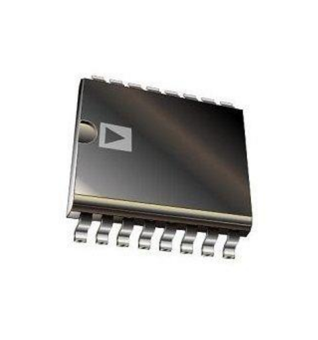
Nexperia 74HC595D Datesheet

The 74HC595; 74HCT595 is an 8-bit serial-in/serial or parallel-out shift register with a storage register and 3-state outputs. Both the shift and storage register have separate clocks. The device features a serial input (DS) and a serial output (Q7S) to enable cascading and an asynchronous reset MR input. A LOW on MR will reset the shift register. Data is shifted on the LOW-to-HIGH transitions of the SHCP input. The data in the shift register is transferred to the storage register on a LOW-to-HIGH transition of the STCP input. If both clocks are connected together, the shift register will always be one clock pulse ahead of the storage register. Data in the storage register appears at the output whenever the output enable input (OE) is LOW. A HIGH on OE causes the outputs to assume a high-impedance OFF-state. Operation of the OE input does not affect the state of the registers. Inputs include clamp diodes.

General description:

The 74HC595; 74HCT595 is an 8-bit serial-in/serial or parallel-out shift register with a storage register and 3-state outputs. Both the shift and storage register have separate clocks. The device features a serial input (DS) and a serial output (Q7S) to enable cascading and an asynchronous reset MR input. A LOW on MR will reset the shift register. Data is shifted on the LOW-to-HIGH transitions of the SHCP input. The data in the shift register is transferred to the storage register on a LOW-to-HIGH transition of the STCP input. If both clocks are connected together, the shift register will always be one clock pulse ahead of the storage register. Data in the storage register appears at the output whenever the output enable input (OE) is LOW. A HIGH on OE causes the outputs to assume a high-impedance OFF-state. Operation of the OE input does not affect the state of the registers. Inputs include clamp diodes. This enables the use of current limiting resistors to interface inputs to voltages in excess of Vcc.

Features and benefits:

• Wide supply voltage range from 2.0 V to 6.0 V

• CMOS low power dissipation

• High noise immunity

• 8-bit serial input

• 8-bit serial or parallel output

• Storage register with 3-state outputs

• Shift register with direct clear

• 100 MHz (typical) shift out frequency

• Latch-up performance exceeds 100 mA per JESD 78 Class II Level B

• Complies with JEDEC standards:

• JESD8C (2.7 V to 3.6 V)

• JESD7A (2.0 V to 6.0 V)

• Input levels:

• For 74HC595: CMOS level

• For 74HCT595: TTL level

• ESD protection:

• HBM: ANSI/ESDA/JEDEC JS-001 class 2 exceeds 2000 V

• CDM: ANSI/ESDA/JEDEC JS-002 class C3 exceeds 1000 V

• Multiple package options

• Specified from -40 °C to +85 °C and from -40 °C to +125 °C

Applications:

• Serial-to-parallel data conversion

• Remote control holding register


How to Order

You can get your Nexperia 74HC595D Datesheet solution by flling out the form below and we will contact you immediately.

Want to turn your idea into reality Contact AXTEK Support
Copyright © 2022 AXTEK Technology Co., Ltd. All Rights Reserved. | Sitemap

Contact

Copyright © 2022 AXTEK Technology Co., Ltd. All Rights Reserved. | Sitemap
Online

Email

Message
TOP