GENERAL DESCRIPTIONS:
The W25N02KV (2G-bit) SLC QspiNAND Flash Memory provides a storage solution for systems with limitedspace, pins and power. The W25N QspiNAND family incorporates the popular SPI interface and thetraditional large NAND non-volatile memory space. They are ideal for code shadowing to RAM, executingcode directly from Dual/Quad SPI (XIP) and storing voice, text and data. The device operates on a single2.7V to 3.6V power supply with current consumption as low as 25mA active, 10µA for standby and 1µA fordeep power down. All W25N QspiNAND family devices are offered in space-saving packages which wereimpossible to use in the past for the typical NAND flash memory.The W25N02KV 2G-bit memory array is organized into 131,072 programmable pages of 2,048-bytes each.The entire page can be programmed at one time using the data from the 2,048-Byte internal buffer. Pagescan be erased in groups of 64 (128KB block erase). The W25N02KV has 2,048 erasable blocks.The W25N02KV supports the standard Serial Peripheral Interface (SPI), Dual/Quad I/O SPI: Serial Clock,Chip Select, Serial Data I/O0 (DI), I/O1 (DO), I/O2 (/WP), and I/O3 (/HOLD). SPI clock frequencies of up to104MHz are supported allowing equivalent clock rates of 208MHz (104MHz x 2) for Dual I/O and 416MHz(104MHz x 4) for Quad I/O when using the Fast Read Dual/Quad I/O instructions.The W25N02KV provides a new Sequential Read Mode that allows for efficient access to the entire memoryarray with a single Read command.A Hold pin, Write Protect pin and programmable write protection, provide further control flexibility.Additionally, the device supports JEDEC standard manufacturer and device ID, one Unique ID page, oneparameter page and ten 2,048-Byte OTP pages. To provide better NAND flash memory manageability, userconfigurable internal ECC is also available in W25N02KV.
FEATURES:
New W25N Family of QspiNANDMemories
– W25N02KV: 2G-bit / 256M-Byte
– Standard SPI: CLK, /CS, DI, DO, /WP,/Hold
– Dual SPI: CLK, /CS, IO0, IO1, /WP, /Hold
– Quad SPI: CLK, /CS, IO0, IO1, IO2, IO3
– Compatible SPI serial flash commands
Highest Performance Serial NAND Flash
– 104MHz Standard/Dual/Quad SPI clocks
– 208/416MHz equivalent Dual/Quad SPI
– 50MB/S sequential data transfer rate
– Fast Program/Erase performance
– 60,000 erase/program cycles
– 10-year data retention
Low Power, Wide Temperature Range
– Single 2.7 to 3.6V supply
– 25mA active, 10µA standby, 1µA DPD(3)
– -40°C to +85°C operating range
Flexible Architecture with 128KB blocks
– Uniform 128K-Byte Block Erase
– Flexible page data load methods
Advanced Features
– On chip 8-Bit ECC for memory array
– ECC status bits indicate ECC results
– Software and Hardware Write-Protect
– Power Supply Lock-Down and OTP protection
– Unique ID and parameter pages(1)
– Ten 2KB OTP pages(2)
Space Efficient Packaging
– 8-pad WSON 8x6-mm
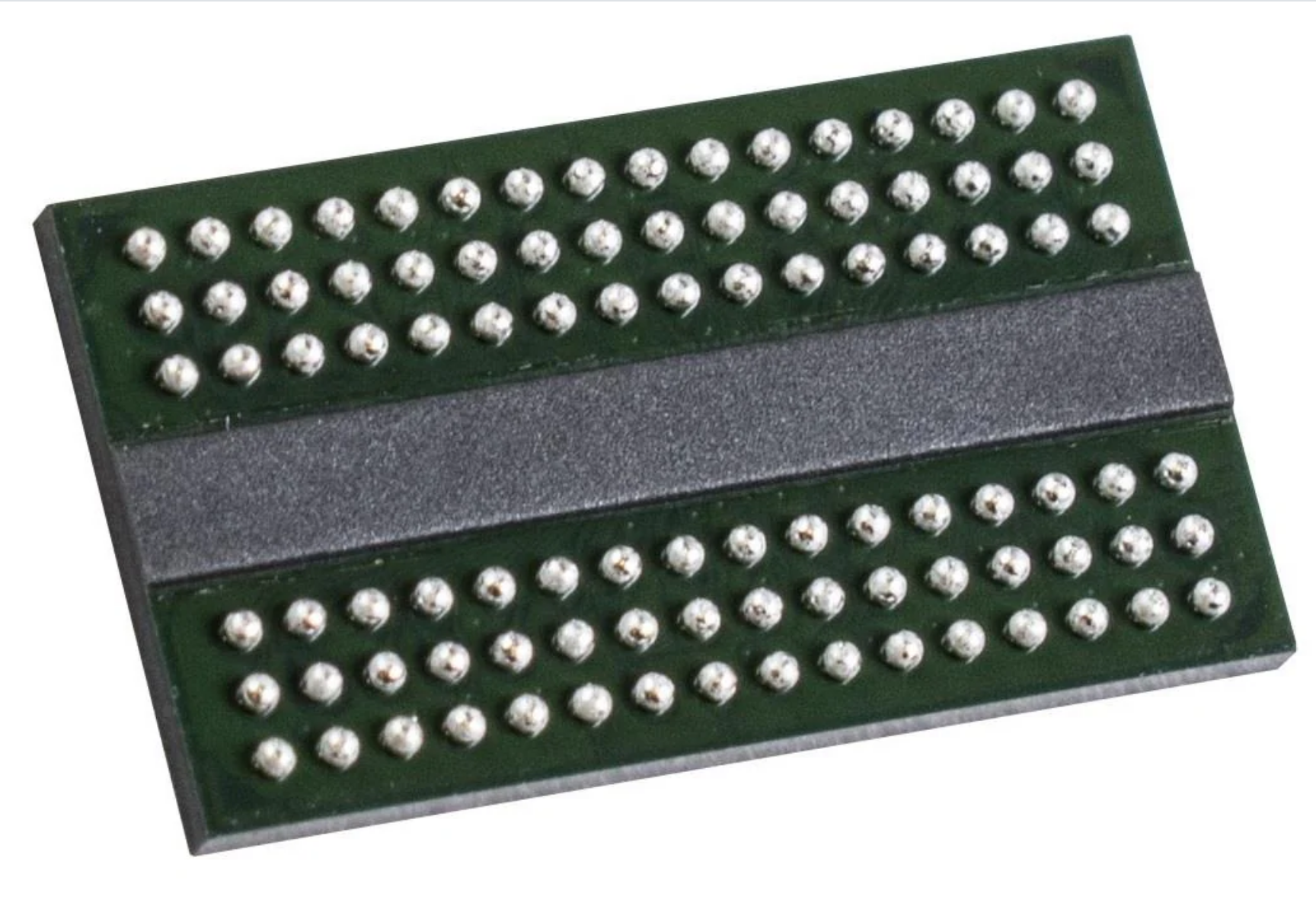
– 24-ball TFBGA 8x6-mm
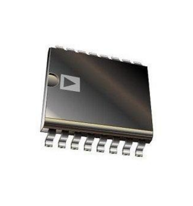
– 16-pin SOIC 300-mil
– Contact Winbond for other package options


 MCU Solutions
 PCBA Solutions
 Bluetooth Solutions
 FAQ
FAQ Contact Us
 Company News
 Technology News
 Industry News
 PCBA News
 Company Profile
 Certificates
 Terms & Conditions
 Privacy Statement
 Home Appliances
 Beauty Appliances
 Lighting
 Kid's Toys
 Security Alarm
 Health Care


