Search...



Description
The TLC6C5912-Q1 is a monolithic, medium-voltage, low-current power 12-bit shift register designed for systems that require relatively moderate load power, such as LEDs. This device contains a 12-bit serial-in, parallel-out shift register that feeds a 12-bit D-type storage register. Data transfer between the shift and storage registers occurs on the rising edges of the shift register clock (SRCK) and the register clock (RCK), respectively. When the shift register clear (CLR) is high, the storage register transfers data to the output buffer. A low level on CLR clears all registers in the device. Holding the output enable (G) high holds all data in the output buffer low and turns off all drain outputs. Holding G low makes the data from the storage register invisible to the output buffer. When the data in the output buffer is low, the DMOS transistor outputs are turned off. When the data is high, the DMOS transistor outputs have current-sinking capability. The serial output (SER OUT) is clocked out of the device on the falling edge of SRCK, providing additional hold time for cascaded applications. This can improve performance for applications where clock signals may be skewed, devices are not located close to each other, or systems with high electromagnetic interference. This device has built-in thermal shutdown protection. The outputs are low-side open-drain DMOS transistors with an output voltage rating of 40 V and a continuous sink-current capability of 50 mA at VCC = 5 V. The current limit decreases as the junction temperature increases, thereby providing additional device protection. The device also provides ESD human-body model protection up to 2000 V and ESD machine-model protection of 200 V. The TLC6C5912-Q1 is rated for an operating ambient temperature range of –40°C to 125°C.
Features:
Qualified for automotive applications
Wide VCC voltage range: 3.5 V to 5.5 V
Maximum output rating of 40 V
12 power DMOS transistor outputs with continuous current output up to 50 mA at VCC = 5 V
Thermal shutdown protection
Enhanced cascading for multiple stages
All registers cleared by a single input
Low power consumption
Slow switching times (tr and tf), which help reduce electromagnetic interference (EMI)
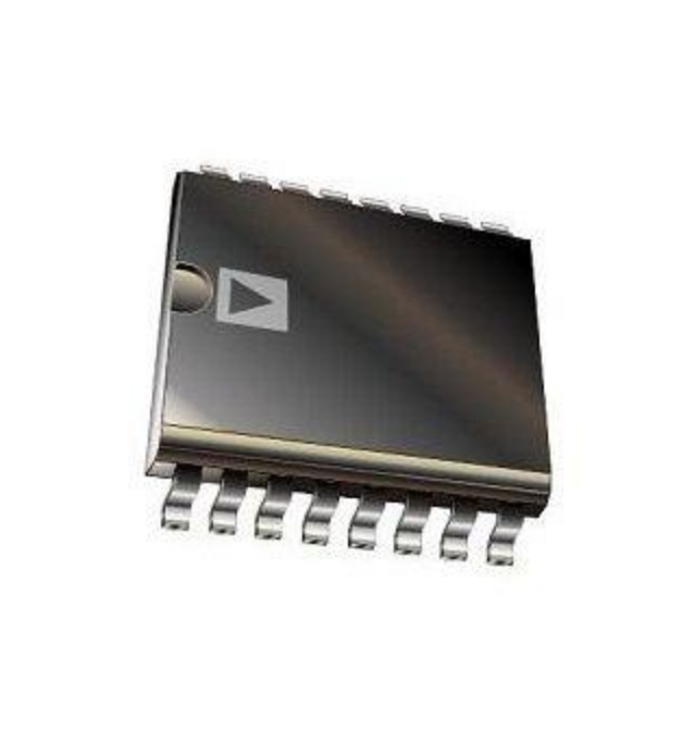
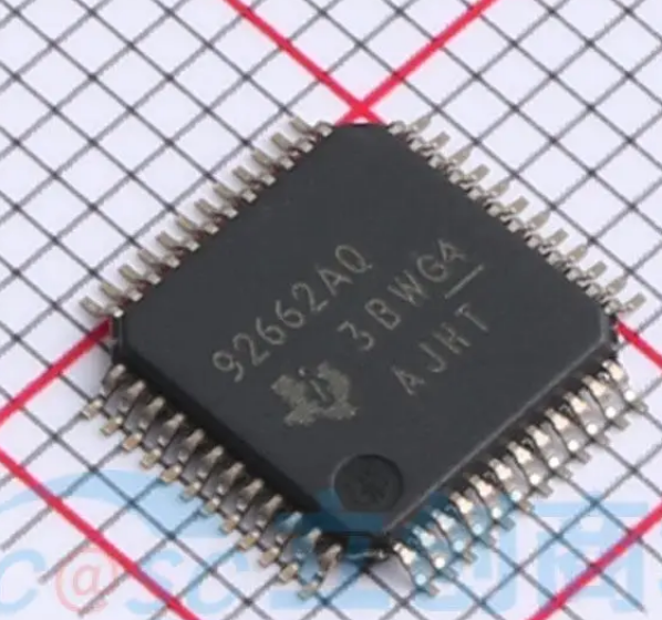
20-pin thin shrink small-outline package (TSSOP)-PW
20-pin DW package
2 Applications
Instrument clusters
Signal lights
LED lighting and control
You can get your TI TLC6C5912QPWRQ1 Datesheet solution by flling out the form below and we will contact you immediately.
AXTEK Series NYQUEST CMSEMICON ST MICROELECTRONICS Featured Manufacturers Puya MCUs ICMAN Touch Chips ZXInfoTek Holtek MCUs MORNSUN Modules
Company Profile Certificates Terms & Conditions Privacy Statement


 MCU Solutions
 PCBA Solutions
 Bluetooth Solutions

 FAQ
 Contact Us

 Company News
 Technology News
 Industry News
 PCBA News

 Company Profile
 Certificates
 Terms & Conditions
 Privacy Statement

 Home Appliances
 Beauty Appliances
 Lighting
 Kid's Toys
 Security Alarm
 Health Care