Description:
The P25Q80L is a serial interface Flash memory device designed for use in a wide variety of high-volume consumer based applications in which program code is shadowed from Flash memory into embedded or external RAM for execution. The flexible erase architecture of the device, with its page erase granularity it is ideal for data storage as well, eliminating the need for additional data storage devices.
The erase block sizes of the device have been optimized to meet the needs of today's code and data storage applications. By optimizing the size of the erase blocks, the memory space can be used much more efficiently.
Because certain code modules and data storage segments must reside by themselves in their own erase regions, the wasted and unused memory space that occurs with large sectored and large block erase Flash memory devices can be greatly reduced. This increased memory space efficiency allows additional code routines and data storage segments to be added while still maintaining the same overall device density.
The device also contains an additional 3*512-byte security registers with OTP lock (One-Time Programmable), can be used for purposes such as unique device serialization, system-level Electronic Serial Number (ESN) storage, locked key storage, etc.
Specifically designed for use in many different systems, the device supports read, program, and erase operations with a wide supply voltage range of 1.65V to 2.0V. No separate voltage is required for programming and erasing.
Overview:
General:
Single 1.65V to 2.0V supply
Industrial Temperature Range -40C to 85C
Serial Peripheral Interface (SPI) Compatible: Mode 0 and Mode 3
Single, Dual and Quad IO mode
- 8M x 1 bit
- 4M x 2 bits
- 2M x 4 bits
Flexible Architecture for Code and Data Storage
- Uniform 256-byte Page Program
- Uniform 256-byte Page Erase
- Uniform 4K-byte Sector Erase
- Uniform 32K/64K-byte Block Erase
- Full Chip Erase
Hardware Controlled Locking of Protected Sectors by WP Pin
One Time Programmable (OTP) Security Register
- 3*512-Byte Security Registers With OTP Lock
128 bit unique ID for each device
Fast Program and Erase Speed
- 2ms Page program time
- 8ms Page erase time
- 8ms 4K-byte sector erase time
- 8ms 32K-byte block erase time
- 8ms 64K-byte block erase time
JEDEC Standard Manufacturer and Device ID Read Methodology
Ultra Low Power Consumption
- 0.1uA Deep Power Down current
- 9uA Standby current
- 1.0mA Active Read current at 33MHz
- 2.0mA Active Program or Erase current
High Reliability
- 100,000 Program / Erase Cycles
- 20-year Data Retention
Industry Standard Green Package Options
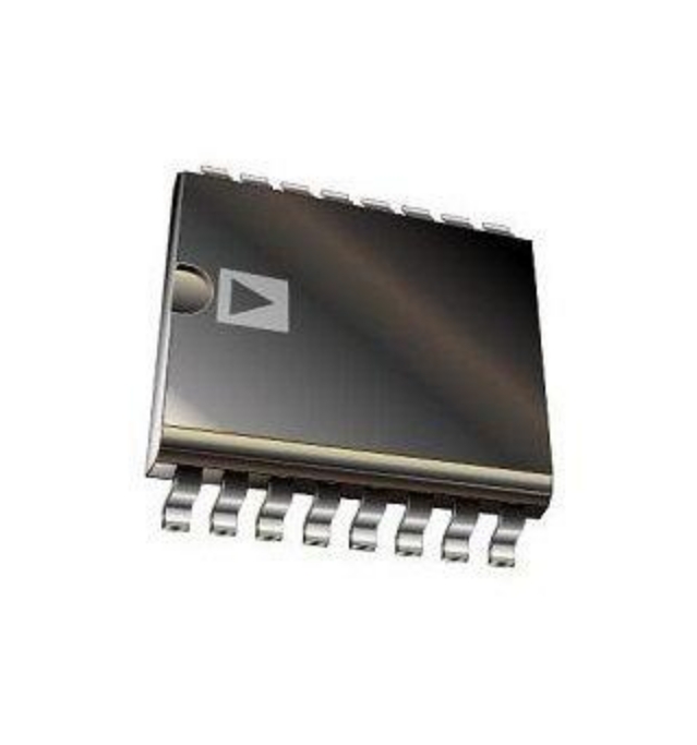
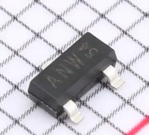
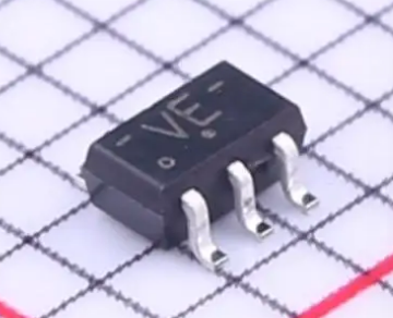
- 8-pin SOP (150mil/208mil)
- 8-land USON (3x2x0.55mm/3x2x0.40m/3x2x0.45mm/3x4x0.55mm)
- 8-land WSON (6x5x0.75mm)
- 8-pin TSSOP
- WLCSP
- KGD for SiP
P25Q80L Datasheet
Puya Semiconductor Page 5 of 70
2 Description


 MCU Solutions
 PCBA Solutions
 Bluetooth Solutions
 FAQ
FAQ Contact Us
 Company News
 Technology News
 Industry News
 Company Profile
 Certificates
 Terms & Conditions
 Privacy Statement
 Home Appliances
 Beauty Appliances
 Lighting
 Kid's Toys
 Security Alarm
 Health Care


