Search...



GENERAL DESCRIPTION:
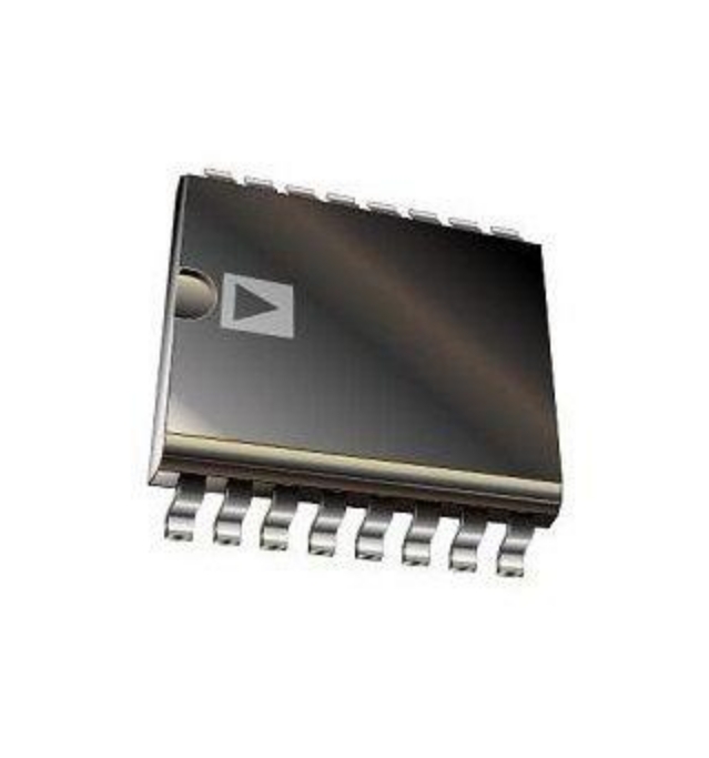
The ADL5902 is a true rms responding power detector that hasa 65 dB measurement range when driven with a single-ended50 Ω source. This feature makes the ADL5902 frequencyversatile by eliminating the need for a balun or any other formof external input tuning for operation up to 9 GHz.The ADL5902 provides a solution in a variety of high frequencysystems requiring an accurate measurement of signal power.Requiring only a single supply of 5 V and a few capacitors, it iseasy to use and capable of being driven single-ended or with abalun for differential input drive. The ADL5902 can operatefrom 50 MHz to 9 GHz and can accept inputs from −62 dBm toat least +3 dBm with large crest factors, such as GSM, CDMA,W-CDMA, TD-SCDMA, WiMAX, and LTE modulated signals.The ADL5902 can determine the true power of a highfrequency signal having a complex low frequency modulationenvelope or can be used as a simple low frequency rmsvoltmeter. Used as a power measurement device, VOUT isconnected to VSET. The output is then proportional to the logarithm of the rms value of the input. In other words, the readingis presented directly in decibels and is scaled 1.06 V per decade,or 53 mV/dB; other slopes are easily arranged. In controller mode,the voltage applied to VSET determines the power level required atthe input to null the deviation from the set point. The outputbuffer can provide high load currents.The ADL5902 has 1.5 mW power consumption when powereddown by a logic high applied to the PWDN pin. It powers upwithin approximately 5 μs to the nominal operating current of73 mA at 25°C. The ADL5902 is supplied in a 4 mm × 4 mm,16-lead LFCSP for operation over the wide temperature rangeof −40°C to +125°C.The ADL5902 is also pin-compatible with the AD8363, 50 dBdynamic range TruPwr™ detector. This feature allows thedesigner to create one circuit layout for projects requiringdifferent dynamic ranges. A fully populated RoHS-compliantevaluation board is available.
FEATURES:
Accurate rms-to-dc conversion from 50 MHz to 9 GHz
Single-ended input dynamic range of 65 dB
No balun or external input matching required
Waveform and modulation independent, such as
GSM/CDMA/W-CDMA/TD-SCDMA/WiMAX/LTE
Linear-in-decibels output, scaled 53 mV/dB
Transfer function ripple: <±0.1 dBTemperature stability: <±0.3 dB
All functions temperature and supply stable
Operates from 4.5 V to 5.5 V from −40°C to +125°C
Power-down capability to 1.5 mW
Pin-compatible with the 50 dB dynamic range AD8363
APPLICATIONS:
Power amplifier linearization/control loops
Transmitter power controls
Transmitter signal strength indication (TSSI)
RF instrumentation
You can get your ADI ADL5902ACPZ Datesheet solution by flling out the form below and we will contact you immediately.
AXTEK Series NYQUEST CMSEMICON ST MICROELECTRONICS Featured Manufacturers Puya MCUs ICMAN Touch Chips ZXInfoTek Holtek MCUs MORNSUN Modules
Company Profile Certificates Terms & Conditions Privacy Statement


 MCU Solutions
 PCBA Solutions
 Bluetooth Solutions
 FAQ
FAQ Contact Us
 Company News
 Technology News
 Industry News
 PCBA News
 Company Profile
 Certificates
 Terms & Conditions
 Privacy Statement
 Home Appliances
 Beauty Appliances
 Lighting
 Kid's Toys
 Security Alarm
 Health Care