Search...



Overview:
The 8A34002 Synchronization Management Unit (SMU) providestools to manage timing references, clock sources, and timingpaths for IEEE 1588 and Synchronous Ethernet (SyncE) basedclocks. The PLL channels can act independently as frequencysynthesizers, jitter attenuators, Digitally Controlled Oscillators(DCO), or Digital Phase Lock Loops (DPLL).Optional clock recovery filter/servo software is available underlicense from Renesas for use with the 8A34002. The filter/servosoftware is designed to suppress the affects of Packet DelayVariation (PDV) on packet based timing signals – it can be usedwith protocol stacks for IEEE 1588 or other packet-based timingprotocols.
Features:
▪ Four independent timing channels
• Each can act as a frequency synthesizer, jitter attenuator,Digitally Controlled Oscillator (DCO), or Digital Phase LockLoop (DPLL)
• DPLLs generate telecom compliant clocks
▪ Compliant with ITU-T G.8262 for Synchronous Ethernet
▪ Compliant with legacy SONET/SDH and PDHrequirements
• DPLL Digital Loop Filters (DLFs) are programmable with cutoff frequencies from 12µHz to 22kHz
• DPLL/DCO channels share frequency information using theCombo Bus to simplify compliance with ITU-T G.8273.2
• Switching between DPLL and DCO modes is hitless anddynamic
▪ Automatic reference switching between DCO and DPLLmodes to simplify support for an external phase/time inputinterface in a T-BC
• Generates output frequencies that are independent of inputfrequencies via a Fractional Output Divider (FOD)
• Each FOD supports output phase tuning with 1ps resolution
▪ 8 Differential / 16 LVCMOS outputs
• Frequencies from 0.5Hz to 1GHz (250MHz for LVCMOS)
• Jitter below 150fs RMS (10kHz to 20MHz)
• LVCMOS, LVDS, LVPECL, HCSL, CML, SSTL, and HSTLoutput modes supported
• Differential output swing is selectable: 400mV / 650mV /800mV / 910mV
• Independent output voltages of 3.3V, 2.5V, or 1.8V
• LVCMOS additionally supports 1.5V or 1.2V
• The clock phase of each output is individually programmablein 1ns to 2ns steps with a total range of ±180°
▪ 7 differential / 14 single-ended clock inputs
• Support frequencies from 0.5Hz to 1GHz
• Any input can be mapped to any or all of the timing channels
• Redundant inputs frequency independent of each other
• Any input can be designated as external frame/sync pulse ofEPPS (even pulse per second), 1 PPS (Pulse per Second),5PPS, 10 PPS, 50Hz, 100Hz, 1 kHz, 2 kHz, 4kHz, and 8kHzassociated with a selectable reference clock input
• Per-input programmable phase offset of up to ±1.638s in1ps steps
▪ Reference monitors qualify/disqualify references depending onLOS, activity, frequency monitoring, and/or LOS input pins
• Loss of Signal (LOS) input pins (via GPIOs) can be assignedto any input clock reference
▪ Automatic reference selection state machines select the activereference for each DPLL based on the reference monitors,priority tables, revertive / non-revertive, and otherprogrammable settings
▪ System APLL operates from fundamental-mode crystal: 25MHzto 54MHz or from a crystal oscillator
▪ System DPLL accepts an XO, TCXO, or OCXO operating atvirtually any frequency from 1MHz to 150MHz
▪ DPLLs can be configured as DCOs to synthesize PrecisionTime Protocol (PTP) / IEEE 1588 clocks
• DCOs generate PTP based clocks with frequency resolutionless than 1.11 × 10⁻¹⁶
▪ DPLL Phase detectors can be used as Time-to-DigitalConverters (TDC) with precision below 1ps
▪ Supports 1MHz I2C or 50MHz SPI serial processor ports
▪ The device can configure itself automatically after reset via:
• Internal customer definable One-Time Programmablememory with up to 16 different configurations
• Standard external I2C EPROM via separate I2C Master Port
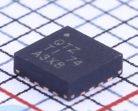
▪ 1149.1 JTAG Boundary Scan▪ 10 × 10 mm 72-VFQFN package
Typical Applications:
▪ Core and access IP switches / routers
▪ Synchronous Ethernet equipment
▪ Telecom Boundary Clocks (T-BCs) and Telecom Time SlaveClocks (T-TSCs) according to ITU-T G.8273.2
▪ 10Gb, 40Gb, and 100Gb Ethernet interfaces
▪ Central Office Timing Source and Distribution
▪ Wireless infrastructure for 4.5G and 5G network equipment
You can get your RENESAS 8A34002E-000NLG Datesheet solution by flling out the form below and we will contact you immediately.
AXTEK Series NYQUEST CMSEMICON ST MICROELECTRONICS Featured Manufacturers Puya MCUs ICMAN Touch Chips ZXInfoTek Holtek MCUs MORNSUN Modules
Company Profile Certificates Terms & Conditions Privacy Statement


 MCU Solutions
 PCBA Solutions
 Bluetooth Solutions
 FAQ
FAQ Contact Us
 Company News
 Technology News
 Industry News
 PCBA News
 Company Profile
 Certificates
 Terms & Conditions
 Privacy Statement
 Home Appliances
 Beauty Appliances
 Lighting
 Kid's Toys
 Security Alarm
 Health Care